Blog
Micro Tactile Switch Trends in Wearables: Low Travel, High Density

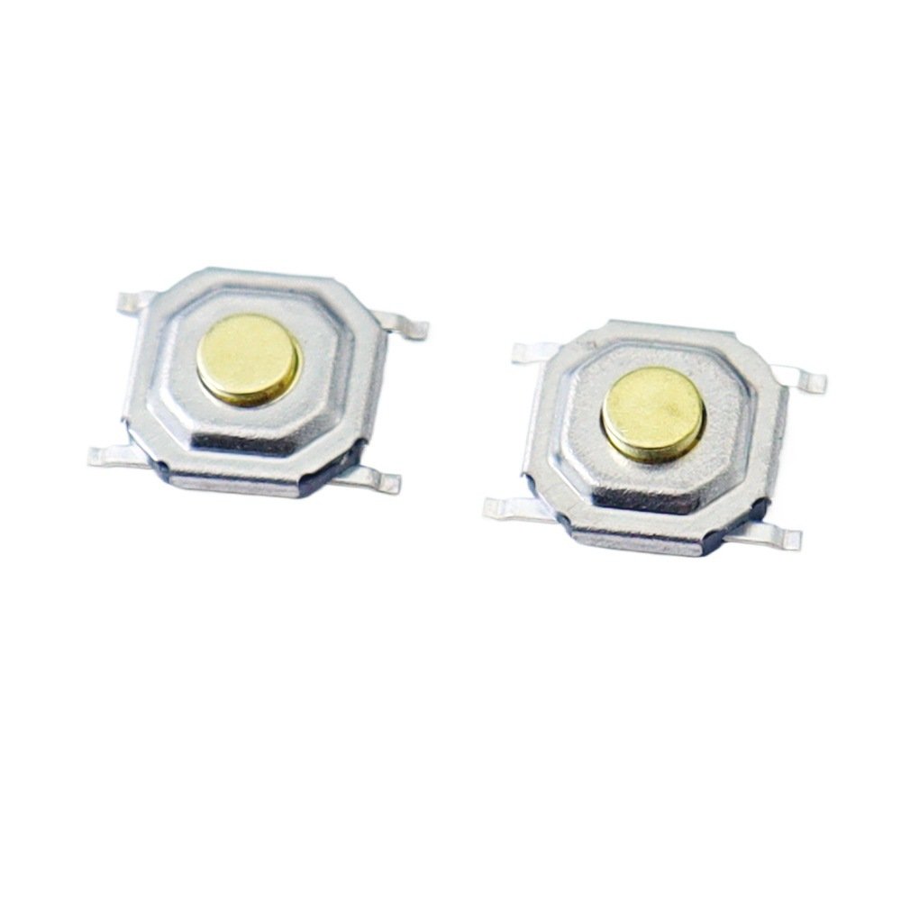
Consumer electronics keep pushing toward thinner, smarter, and more integrated designs. That movement creates real opportunities and hard constraints for micro tactile switches, which serve as primary input components in finished devices. Wearables such as smartwatches and TWS earbuds demand extreme limits on size, weight, interaction feel, and reliability. The same pressure applies to small portable products including styluses, mini remote controls, and health monitoring devices.
This article examines where micro tactile switch technology is heading in these products. It focuses on low-travel design, high-density placement, structural innovation, and integrated modules. Real application scenarios come first, because the design constraints differ sharply between an earbud button and a smartwatch crown. For engineers and sourcing teams, understanding these trends means selecting the right switch family earlier and avoiding late-stage redesigns.
Market Drivers: Miniaturization Meets User Experience
Wearables and compact portable electronics continue to grow, and component requirements keep escalating in parallel. Four demands define the current landscape.
Limited space. Many products stay under 10 mm in thickness, leaving very little room for any switch assembly.
Low weight. A single device often needs to stay below 0.1 g while still withstanding frequent operation.
High reliability. Designs must pass hundreds of thousands of operating cycles and resist sweat, humidity, and drop shock.
High integration. Buyers increasingly expect one module to combine press feedback, light piping, sealing, and signal transmission.
Micro tactile switches suit these requirements well. Their compact structure, clear tactile feel, fast response, and controllable cost make them the default input choice for most wearable and portable designs. For a full view of available sizes and stroke options, our complete guide to micro tactile switch specifications covers everything from 3 mm to 12 mm.
Application Evolution in Earbuds and Smartwatches
Side-Buttons in TWS Earbuds
TWS earbuds represent the most demanding portable category. Requirements are strict. The control must stay small and sensitive without disrupting the housing shape. Feedback should feel clear, yet travel must stay extremely short at under 0.2 mm. The part must also resist sweat, drops, and accidental presses.
Design trends reflect those constraints. Ultra-low-profile structures have thinned from 1.5 mm down toward 0.6 mm, with some designs using a film type without a top cap. Protection levels have also risen, and some manufacturers now adopt IP67 sealed tactile switches so sweat cannot affect the assembly after the earbud is built. Light piping adds a further function, since an LED indicator can share the switch position through a center hole or bypass light guide structure.
As an example, one international TWS brand integrates a 3.0 × 2.6 × 0.65 mm tactile switch inside the housing. It attaches through FPC soldering and supports volume adjustment plus voice-assistant wakeup. The same part also works alongside capacitive touch, giving users both mechanical and touch input modes.
Multifunction Side Buttons in Smartwatches
Smartwatch side controls, including digital crowns and function keys, often combine several operations. They handle input, menu navigation, mode switching, and lighting control in one physical space.
Several challenges appear. Edge thickness stays at 10 mm or below, so switch height must remain under 1 mm. Skin contact demands corrosion and sweat resistance. Users press these controls heavily, so life expectancy of at least 100,000 presses matters. Dense circuit placement raises the bar for package stability as well.
Technology development follows those limits. Low-travel feel optimization upgrades the spring material, tunes micro guide posts, and refines the top cap shape to reach under 0.15 mm travel while keeping clear feedback. Integrated switch and knob modules combine a tactile switch with an encoder or wheel to save space. EMI shielding adds a nickel-plated shield layer or metal backplate so high-frequency wireless signals do not disturb the circuit.
Apple Watch illustrates the approach. Its Digital Crown uses a central tactile feedback structure paired with a magnetic rotary encoder, which delivers precise input and a well-tuned tactile experience.
Core Trends in Micro Tactile Switch Development
Shorter Travel with Clearer Feedback
The industry continues to move toward ultra-short travel and crisp rebound. Achieving a distinct feel at very small displacement is the core challenge. Engineers use oval corrugations, stepped spring leaves, precision stamping, and thin guide post designs to reach it.
High-Density Packaging: Multiple Switches per Board
Space constraints mean one FPC board often carries 4 to 8 tactile switches, and each one must operate without interference. Several techniques make this work. Unified pad design and precision placement guides improve assembly efficiency. EMC layout keeps signal traces separate from power traces to prevent interference. Backside mounting places switches on the rear of an FPC or two-sided PCB, which saves front-side area. LGA leadless packages enable fully surface-mount designs and reduce overall thickness.
PCB layout also decides whether high-density placement works in practice. Our guide to micro tactile switch footprint selection compares top-actuated and side-actuated options and the layout trade-offs that follow.
Functional Module Integration
A modern micro tactile switch is no longer a single component. It increasingly integrates additional functions. An integrated LED or light guide column provides status feedback and backlighting. A pressure sensing membrane works with the MCU to recognize press force. A metal cover plate merges the housing with the switch structure and cuts part count. Integrated sealing uses a silicone gasket or nano waterproof coating to reach IPX7 for the whole assembly.
This trend delivers higher integration, smaller volume, and faster assembly, which makes it a defining direction for the next generation of tactile switch design.
Technical Challenges and Solutions
miniaturization also creates engineering trade-offs. The table below lists the main challenges and the methods that address them.
| Technical Challenge | Description | Solution |
|---|---|---|
| Conflict between miniaturization and reliability | Smaller dimensions mean shorter travel and more fragile springs | Use high-elasticity stainless steel and optimize precision stamping |
| Durability under high-frequency use | Wearables require up to one million operation cycles | Upgrade the spring design and use thicker silver-plated contacts for stable conduction |
| High waterproof and dustproof requirements | Limited space leaves little room for sealing | Apply silicone gaskets or conformal coating plus full potting encapsulation |
| Signal interference risk | High-frequency wireless signals can disturb the circuit | Strengthen EMI design, separate PCB traces, and add electromagnetic shielding |
Future Directions
Flexible Bendable Switch Modules
Smart garments and curved wearables demand input solutions that bend. Micro tactile switches will increasingly use flexible FPC platforms with deformable housings, creating bendable structures that fit curved surfaces.
Smart Recognition Switches
Combining microcontrollers with AI edge algorithms allows switches to recognize different press forces, frequencies, and patterns. That capability supports richer human-machine interaction.
Standardized Modules
Micro tactile switches will stop being loose parts. Platform-based standardization turns them into functional input modules with unified interfaces, dimensions, and electrical specs, which lets OEM teams adopt them quickly.
Conclusion
Micro tactile switches have become decisive components for wearable and portable devices. Their path toward smaller size, faster response, and greater integration leads the entire input component industry into a new stage. For product developers, a clear grasp of these trends and the right component choice improves competitiveness and shortens design cycles. For switch manufacturers, continuous work on miniaturization, reliability, and integration remains the only way to hold a position in the next wave of smart hardware.